The figure depicts a basic architecture of a desktop computer available in the late 1970s. The architecture is simple but still representative of the contemporary desktop computers. Advances in the architecture since 1970s are outlined in the subsequent sections.
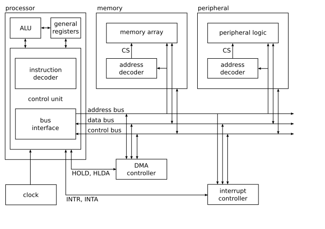
At the core of the architecture is the control unit of the processor. In steps timed by the external clock signal, the control unit repeats an infinite cycle of fetching a code of the instruction to be executed from memory, decoding the instruction, fetching the operands of the instruction, executing the instruction, storing the results of the instruction. The control unit uses the arithmetic and logic unit to execute arithmetic and logic instructions.
The control unit of the processor communicates with the rest of the architecture through a processor bus, which can be viewed as consisting of three distinct sets of wires denoted as address bus, data bus and control bus. The address bus is a set of wires used to communicate an address. The data bus is a set of wires used to communicate data. The control bus is a set of wires with functions other than those of the address and data buses, especially signals that tell when the information on the address and data buses is valid.
The exact working of the processor bus can be explained by a series of timing diagrams for basic operations such as memory read and memory write.
What all operations of the processor bus have in common is the general order of steps, which typically starts with the processor setting an address on the address bus and a signal on the control bus that indicates presence of a valid address, and proceeds with the transfer of data. Any device connected to the processor bus is responsible for recognizing its address, usually through an address decoder that sends the chip select signal when the address of the device is recognized.
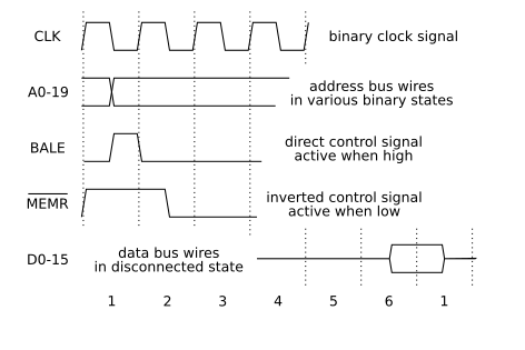
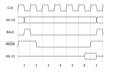
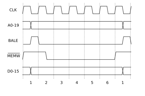
The ISA (Industry Standard Architecture) bus is synchronized by a clock signal ticking with the frequency of 8-10 MHz. In the first clock tick of a bus cycle, the bus master, which is typically the processor, sets the address on the address bus and pulses the BALE (Bus Address Latch Enable) signal to indicate that the address is valid.
In a read bus cycle, the bus master activates one of the MEMR (Memory Read) or IOR (Input/Output Read) signals to indicate either reading from memory or reading from an input device. The bus master waits the next four cycles for the memory or the device to recognize its address and set the data on the data bus.
In a write bus cycle, the bus master activates one of the MEMW (Memory Write) or IOW (Input/Output Write) signals to indicate either writing to memory or writing to an output device. The bus master sets the data on the data bus and waits the next four cycles for the memory or the device to recognize its address and data.
To provide means of requesting attention from outside, the processor is equipped with the interrupt and interrupt acknowledge signals. Before executing an instruction, the control unit of the processor checks whether the interrupt signal is set, and if it is, the control unit responds with setting the interrupt acknowledge signal and setting the program counter to a predefined address, effectively executing a subroutine call instruction.
To better cope with situations where more devices can request attention, the handling of the interrupt request signal is delegated to an interrupt controller. The controller has several interrupt request inputs and takes care of aggregating those inputs into the interrupt request input of the processor using priorities and queuing and providing the processor with information to distinguish the interrupt requests.
To provide means of transferring data without processor attention, the processor is equipped with the hold and hold acknowledge signals. The control unit of the processor checks whether the hold signal is set, and if it is, the control unit responds with setting the hold acknowledge signal and holding access to the processor bus until the hold signal is reset, effectively relinquishing control of the processor bus.
To better cope with situations where more devices can transfer data without processor attention, the handling of the hold signal is delegated to a direct memory access controller. The controller has several transfer request inputs associated with transfer counters and takes care of taking over the processor bus and setting the address and control signals during transfer.
The ISA (Industry Standard Architecture) bus DMA cycle is commenced by the peripheral device requesting a transfer using one of the DRQ (DMA Request) signals. There are 4 or 8 DRQ signals, DRQ0 to DRQ3 or DRQ7, and 4 or 8 corresponding DACK (DMA Acknowledge) signals, DACK0 to DACK3 or DACK7, each associated with one set of transfer counters in the controller.
When the controller sees the peripheral device requesting a transfer, it asks the processor to relinquish the bus using the HRQ (Hold Request) signal. The processor answers with the HLDA (Hold Acknowledge) signal and relinquishes the bus. This typically happens at the end of a machine cycle.
Once the bus is not used by the processor, the controller performs the device-to-memory or memory-to-device bus transfer in a manner that is very similar to the normal processor-to-memory or memory-to-processor bus transfer. The controller sends the memory address on the address bus together with the AEN (Address Enable) signal to indicate that the address is valid, responds to the peripheral device requesting the transfer using one of the DACK signals, and juggles the MEMW and IOR or the MEMR and IOW signals to synchronize the transfer.