The operations of the processor bus were optimized for the common case of transferring a block of data from consecutive addresses. Rather than setting an address on the address bus for each item of the block, the address is only set once at the beginning of the transfer and the block of data is transferred in a burst.
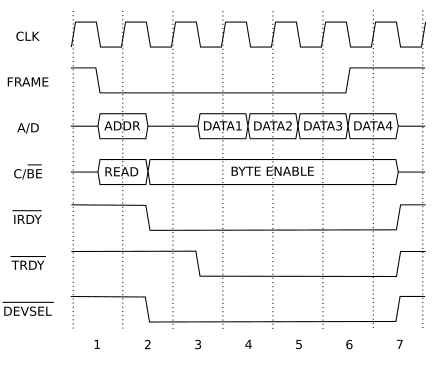
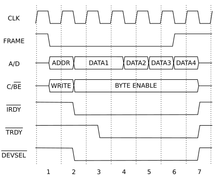
The PCI (Peripheral Component Interconnect) bus transfers multiple units of data in frames. A frame begins with transporting an address and a command that describes what type of transfer will be done within the frame. Next, data is transferred in bursts of limited maximum duration.
In a single bus cycle, the bus master activates the FRAME signal to denote the start of the cycle, sets the C/BE (Command / Byte Enable) wires to describe the type of transfer (0010 for device read, 0011 for device write, 0110 for memory read, 0111 for memory write, etc.) and sets the A/D (Address / Data) wires to the address to be read from or written to.
After the address and the command is transferred, the bus master uses the IRDY (Initiator Ready) signal to indicate readiness to receive or send data. The target of the transfer responds with DEVSEL (Device Select) to indicate that it has been addressed, and with TRDY (Target Ready) to indicate readiness to send or receive data. When both the initiator and the target are ready, one unit of data is transferred each clock cycle.
Note that there are many variants of the PCI bus. AGP (Accelerated Graphics Port) is based on PCI clocked at 66 MHz and doubles the speed by transporting data on both the rising and the falling edge of the clock signal. PCI-X (Peripheral Component Interconnect Extended) introduces higher clock speeds and ECC for error checking and correction.
Multiprocessor systems and complex devices do not fit the concept of a single processor controlling the processor bus. An arbitration mechanism is introduced to allow any device to request control of the processor bus. (PCI has an arbitrator who can grant the use of the bus to any connected device.)
The ISA (Industry Standard Architecture) bus DMA cycle can be extended to support bus mastering. After the controller finished the DRQ and DACK handshake, the peripheral device could use the MASTER signal to request bus mastering. The controller responded by relinquishing control of the bus to the peripheral device. Although not typical, this mechanism has been used for example by high end network hardware.
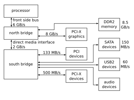
The speed of the processor differs from the speed of the memory and other devices. To compensate for the difference, multiple buses are introduced in place of the processor bus from the basic architecture described earlier. (PC has a north bridge that connects processor to memory and graphic card on AGP at one speed and to south bridge at another speed, and a south bridge that connects integrated devices to north bridge at one speed and PCI slots at another speed.)